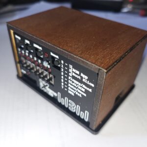
Hi, Hope you are enjoying EMF CAMP.
If you are here, the chances are you have just met Derek and Extreme Kits.
More details on the badge…
The challenge
Everyone makes a Badge for events that usually contains a microprocessor, a display and some blinking lights. I wanted something different. Retro and of course it must work as a badge.
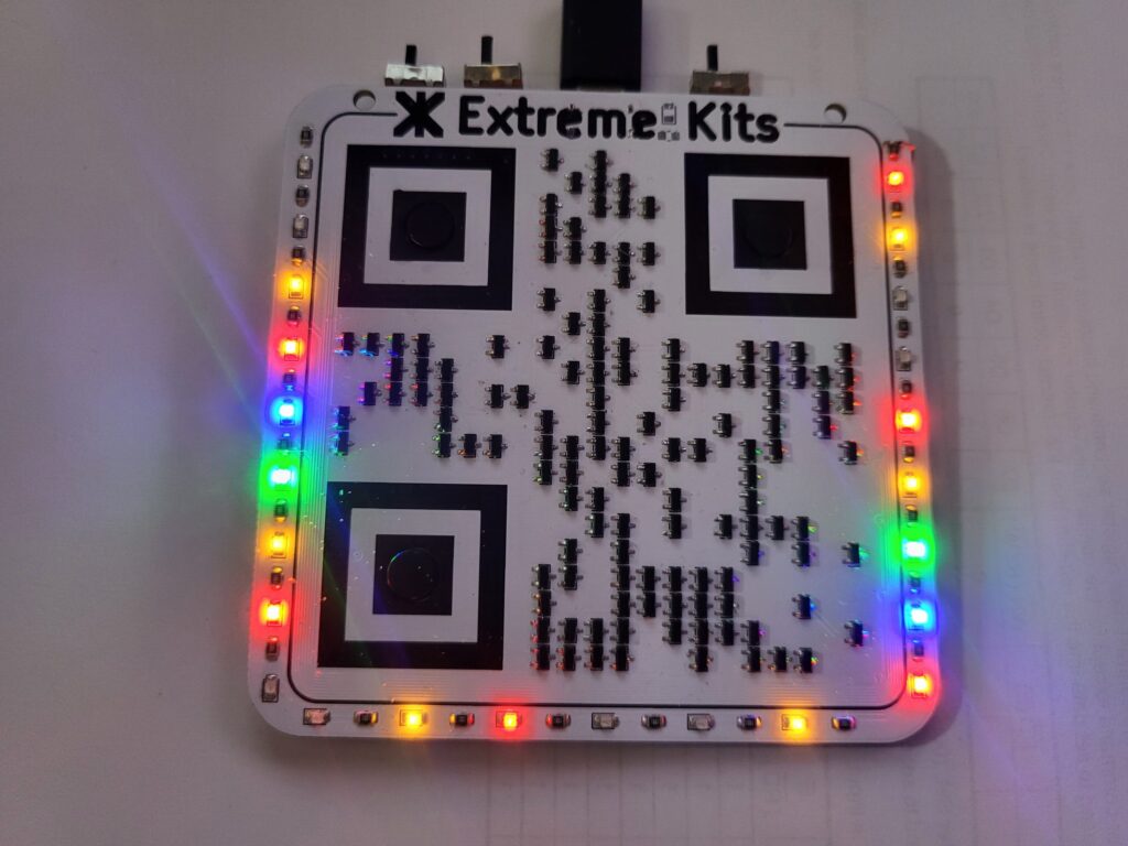
So I wanted to have something retro and something with a QR code, so It could be easily linked back to Extreme Kits. The challenge was born, I want to make a working electronic badge, where the components are the black blobs in the QR code. Simple 🙂 …
The Badge
What it does
Primarily it needs to serve as a badge for Extreme kits, The QR code is the most important thing. But it needs to be fun, different and attractive (probably not that pretty though).
What it actually does, the QR code is made from 3 buttons (the targets) and 134 MOSFETs, with a bit of help from the PCB silkscreen. The MOSFETs form an 11 stage shift register, that drives the 24 coloured LEDs around the outside of the badge.
Why?
As a badge, It needs to be different, to stand out. Everyone does badges with microprocessors and displays. Plus, I thought it would be easy 🙂
Building the Badge
The QR Code
QR codes come in a range of sizes and types, but whatever I choose, it must be easily recognisable by most mobile devices. It also must be able to encode a workable https web site address. Micro QR codes were my first thought, but these are not easily recognisable by phones and also have only a small capacity of 15 bytes. The rectangular versions may have worked, but I don’t think these work well where a mostly portrait (phone) will be taking the picture.
I decided on the version 2 variant, which is a grid of 25×25 dots with three position alignment areas (square targets), until I realised that that indicated 625 dots, assuming half of them would need to be “black” then 313 components. (including the targets)
After some experiments I found that phones would fail to capture QR codes where the targets weren’t continuous, so I had to have some component feature that wouldn’t break these into dots.
Even with removing the targets (each 7 square) from my component count that only reduced the component count by (7x7x3/2) 74 components, which still left well over 200 components.
So I looked again at version 1. The advantage of version 1 is it’s 21×21 which is “only” 441 blobs, again removing the targets and assuming only half will need to be black gives (441-74)/2= ~183 and there is an enforced white area around each target dropping this figure down to ~143, much more manageable.
Until I tried to create a https web address. “http://extkits.co.uk” is 21 characters. Version 1 will only allow 17 if you include non-alphanumeric characters (binary) and have some error correction. Unfortunately the : and // are quite important in a web address. (https://www.qrcode.com/en/about/version.html)
So as I really didn’t want to solder in a huge amount of components I registered the domain xkts.uk giving me a URL of “https://xkts.uk“, which is then redirected here.
So I settled on Version 1 21×21 modules(blobs) with Low Error Correction. At only 143 blobs (excluding targets) definitely doable.

The Targets
With further consideration, I thought the targets were a cop-out. But no combination of components would allow consistent detection without sharply defined lines. So eventually, I put 12mm tactile push buttons in the centre of each target so the target is the actual button.
Components
To fit into the QR code, unless it was going to be huge, the components must be relatively small, for a 100mm square badge each component must be no more than 4.7mm square to get 21 of them (and a border) in a row. This meant the only option would be surface mount.
Looking at various components my first thought was to make a circuit with surface mount transistors, resistors and capacitors. A quick trial pointed out some issues. Surface mount capacitors aren’t black, you can colour them black, but I really didn’t want to paint tens of components. Surface mount resistors are, mostly black, apart from the values painted on them. But both resistors and capacitors have large shiny metal ends.
Transistors however have a mostly black case, and small contacts in comparison with their size the only down side is they are long and thin, but as long as they are centred to the required area QR codes are quite happy with this. Plus they are roughy 3mm square (including legs) well within the 4.7mm maximum dictated by the PCB size.
Return of the Retro theme
So, I need an electronic design that will flash some LED’s with a large number of transistors and not many other components. Mosfet Logic fits right into this nicely.
Digital Integrated Circuits are all just many transistors squished into a silicon circuit and encapsulated in a plastic block and wired out as inverters, logic gates, registers, adders and microprocessors. ( greatly simplified, don’t @ me)
We have loads of transistors, we can do this the old way. I’m going to use Field Effect Transistors mostly because they are cheap.
FET Logic Primer
The FET
An FET is a switch
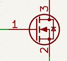
With this FET, an N-type, with 0 volts on the gate (1) the Drain(3) and the Source(2) will not be connected.
If you put a few volts +ve on the gate(1), the Drain(3) and the Source(2) will be connected.
There is also another type of FET, also a switch (note the arrow direction has changed on the symbol).
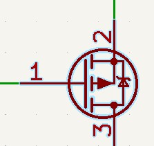
With this FET, a P-type, with 0 volts on the gate (1) the Drain(2) and the Source(3) will be connected.
If you put a few volts on the gate(1), the Drain(2) and the Source(3) will be disconnected.
(The P-type is actually an upside down N-type and you are actually putting -ve volts on the gate with respect to the source, but that makes the rest of the descriptions below really hard. https://en.wikipedia.org/wiki/Field-effect_transistor for more information)
The Inverter or NOT .
So, we can make the simplest type of logic gate with transistors, an inverter or NOT gate.
A NOR gate has one input and one output. A HIGH(1) on the input will give a LOW(0) on the output, and a LOW(0) on the input will make a HIGH(1) on the output.
| In | Out |
|---|---|
| 0 | 1 |
| 1 | 0 |
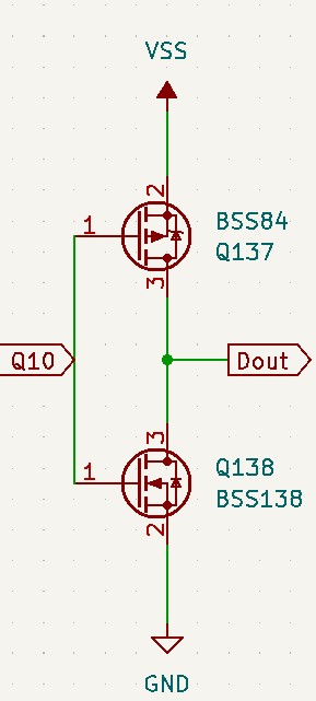
So, from the above description, If the input (Q10) it at GND (LOW), the bottom transistor (n-type) is OFF and the Top transistor(p-type) is ON.
As the top transistor is connected to VSS (HIGH) the output (Dout) is HIGH.
Making Q10 HIGH, Turns on the Bottom transistor which is connected to GND, and turns off the top transistor. So the output is LOW.
Confused. Yes, I have to think about this hard every time I come across it.
One thing to take from this simple example is, if you only have one transistor between the input and the output, the signal will be inverted.
This is the reason that all of the basic gates made from transistors are in their inverted forms, NAND, NOR etc, as you need another pair of transistors to invert the output again, to make the gates their non inverted counterparts OR and AND.
For more details on the way logic gates work take a look at this great guide https://www.geeksforgeeks.org/digital-logic/logic-gates/
From here, we can make all of the classic Gates, NOR,NAND and with the addition of an inverter gate as above OR and AND gates.
NAND (Not AND)
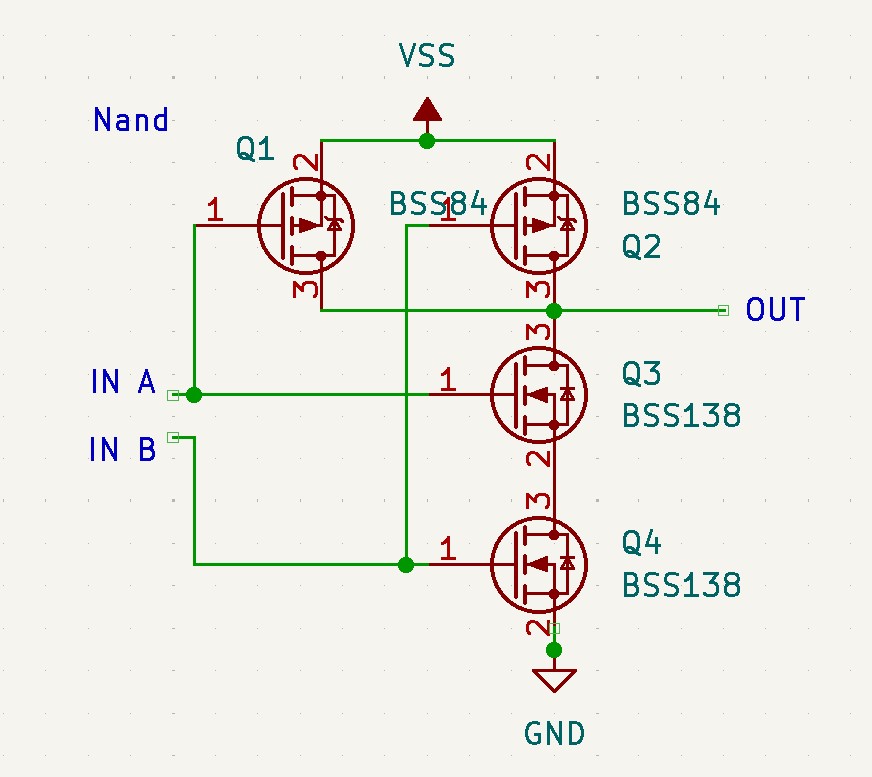
The NAND gate is slightly more complicated having two inputs and one output.
| A | B | OUT |
|---|---|---|
| 0 | 0 | 1 |
| 1 | 0 | 1 |
| 0 | 1 | 1 |
| 1 | 1 | 0 |
As Q3 and Q4 are N-Type only If both of the transistors have a HIGH(1) on their input, then the output will be pulled LOW(0). If either of the P-Type transistors Q1 and Q2 have a LOW(0) on their input then the output will be pulled HIGH(1)
NOR (Not Or)
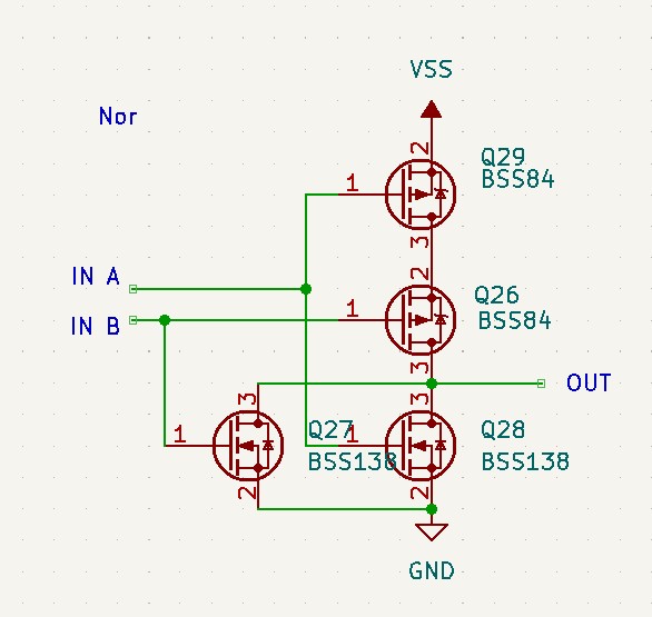
The NOR gate is similar also having two inputs and one output.
| A | B | OUT |
|---|---|---|
| 0 | 0 | 1 |
| 1 | 0 | 0 |
| 0 | 1 | 0 |
| 1 | 1 | 0 |
As Q27 and Q28 are N-Type If ether of the transistors have a HIGH(1) on their input, then the output will be pulled LOW(0). If both of the P-Type transistors Q26 and Q29 have a LOW(0) on their input then the output will be pulled HIGH(1)
That’s great, but logic gates don’t flash LED’s.
OK to start flashing things we need an oscillator. My first thought was an NE555 (or course) but that’s way too predictable, and hey, we are trying to use transistors. The second thought was to make a 555 out of transistors, which of course is doable. (https://xtronic.org/circuit/build-discrete-555-timer-using-transistor-diy/) but actually, really complicated, and I wanted a chance of getting this working. So, a multi-vibrator will do and is relatively simple, therefore likely to work…
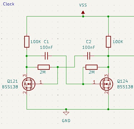
I think this astable-multi-vibrator circuit is iconic enough to not warrant explanation. (https://en.wikipedia.org/wiki/Multivibrator). The only thing to note here is the high resistance values, Yes FET’s gates are really sensitive.
This gives me a clock of around 2 Hz.
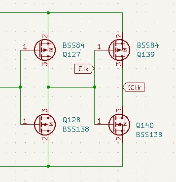
I feed the clock to the shift register using this circuit, this does three things, It isolates the clock from the oscillator, gives a high current drive for the 40 or so gates it will need to drive, and gives me Clock (Clk), and inverted Clock (!Clk) so I don’t need to duplicate this for the other elements in the circuit.
The output of this oscillator will flash two LED’s, but we are not nearly using enough transistors and 2 LED’s isn’t that impressive, So….
The D-Type Latch
So, I needed to control a bunch of LEDS, my thought was a shift register. My idea was, if we make a long shift register from D-Type latches we can feed in a string of on’s and off’s, and it can filter through the shift register driving the LEDs. (https://www.geeksforgeeks.org/digital-logic/shift-registers-in-digital-logic/)
So First, I needed a D-type latch circuit
This is the second circuit I tried, the first, from a very respectable internet source was not even wrong, yes that bad, and I didn’t check it, until I had some PCB’s made. The lesson here is, never believe what you read on the internet regardless of source 🙂
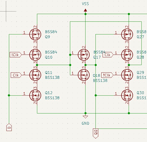
Anyway, this takes a high or low (1, or 0) signal ‘D’, and stores it’s state at ‘Q0’ when there is a +ve going clock ‘Clk’. You can see that this circuit also uses the inverted clock ‘!Clk’.
For a 10 transistor circuit, it’s operation is really quite complicated. But basically on a +ve clock ‘D’ is connected to MOSFETs Q17 and Q18, setting the output ‘Q0’, this is latched during a -ve going clock by the MOSFETs Q27,Q28,Q29 and Q30 and the feedback loop back to MOSFETs Q17,Q18.
This works fine, but if you connect another d-type as above, connecting the new D to the output Q0, the signal gets latched immediately on the +ve going clock, so all subsequent D-types latch ‘on’ with the first clock transition, not what I want.
The solution, is to alternate a +ve latching D-type latches with a -ve latching D-type latches. This is easily achieved by swapping the ‘Clk’ and ‘!Clk’ signals in the second latch.
So these 20 transistors form 2 latches in a shift register. If we connect the LEDs to these outputs we get running lights.
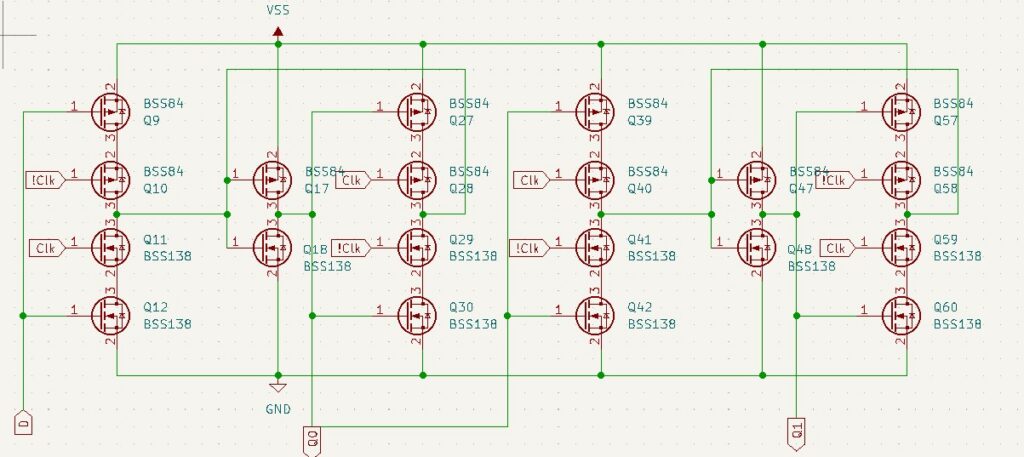
The badge has 5.5 of these stages. which take up most of the required 134 transistors to make the QR code.
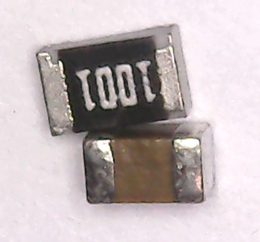
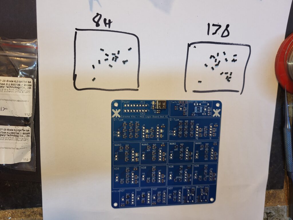
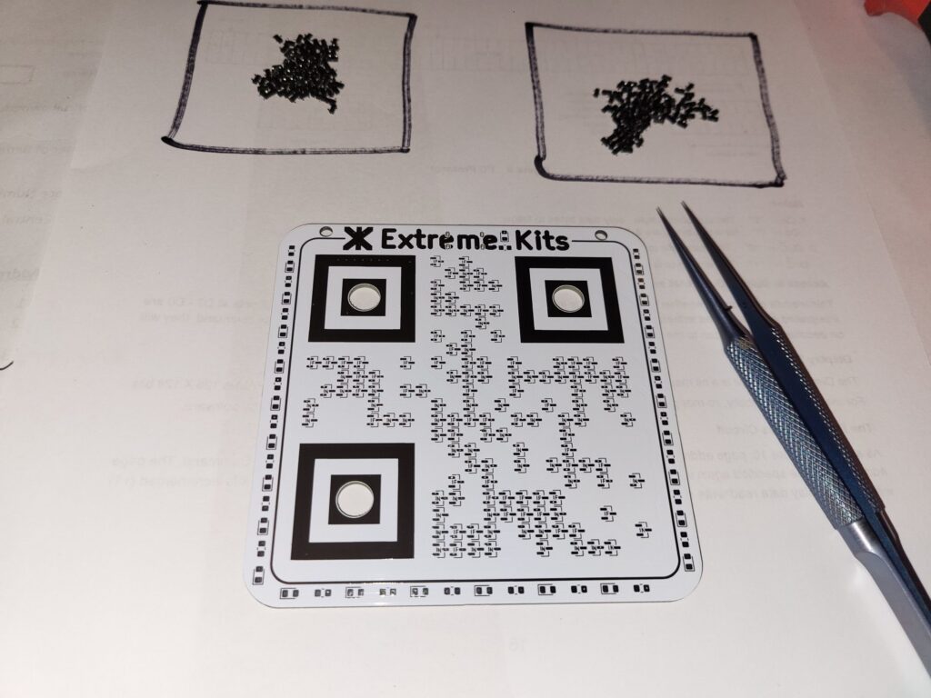
As I hadn’t played with any of this MOSFET gate theory since I was in college, and that was last century (literally). So I made a test PCB with some of my ideas before committing to the “real PCB”. This is my sheet for the placing of the transistors in the test PCB, the ’84’ are the P-Type MOSFETs and the 138’s are the N-Type.
It mostly worked, but this was how I found out the circuit for the d-type latch was incorrect, so I had to make another small batch of PCB’s to prove the replacement circuit too. I also made these white so I had a reference for the final design.
Here they are, with a proof of concept 6 stage shift register.
and a real bodge up PCB to test the astable multi-vibrator oscillator circuit with my Nano Probe.
One thing these tests also told me is, don’t ever leave gates floating, the inverter circuit and the gates in the PCB (above) will happily sit with it’s inputs at half voltage, turning on both transistors and shorting out the power of nothing is connected to their inputs.
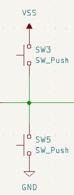
Switches
There are three switches at the top of the badge, these are power, (technically battery/USB). Clock source (switches between manually clocked and oscillator), and Feedback (how the end of the shift register is connected to the beginning).
Feedback switches between an inverter from the last LED to the first, and to the output of the XOR gate that will give a random sequence of 1’s and 0’s. (see below)
Buttons
The three buttons are placed in the three targets, two allow forcing 0’s and 1’s into the shift register, abd a third is used to manually clock the shift register.
XOR – Random
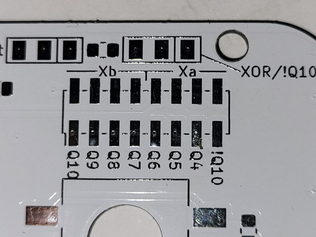
With the switch in the random position, selected shift register outputs are XOR’d together to provide an input to the shift register, this provides a psudo-random sequence of a length determined by the feed back settings.
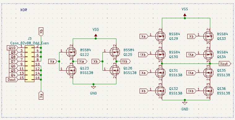
The XOR feedback is selected by the 16 way solder block on the back of the device, the top is split in to two sets of four, these are the two inputs to the XOR gate, the other 8 are Q4 to Q10 from the shift register and an inverted Q10 (Dout).
Layout
I use KICAD (PCB layout program) its flexibility for this was essential.
To test the initial concept I made a 3D render of the PCB to ensure that the QR code would work.
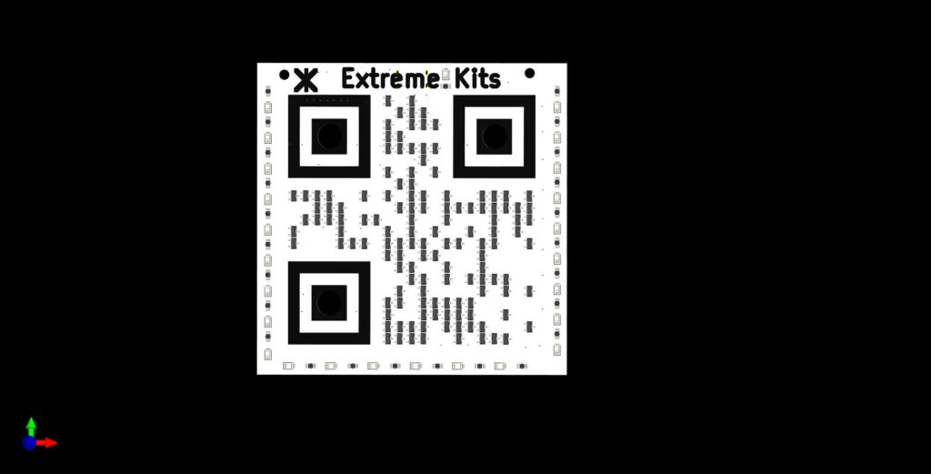
This was a vital check, if this didn’t work the project was dead in the water. The ability to change the colours of the rendered PCB layers also proved that it needed to be a white PCB as other (cheaper) colours would not give me the contrast and a reliable QR code.
After placing a few tens of transistors, the simplicity of the footprint on the PCB became important too, in the end I scrapped all information except N and P on the transistor as that is all I needed to know when populating the circuit, although the ‘P’s are cut into by the pads, remember these MOSFETs are ~3mm square.
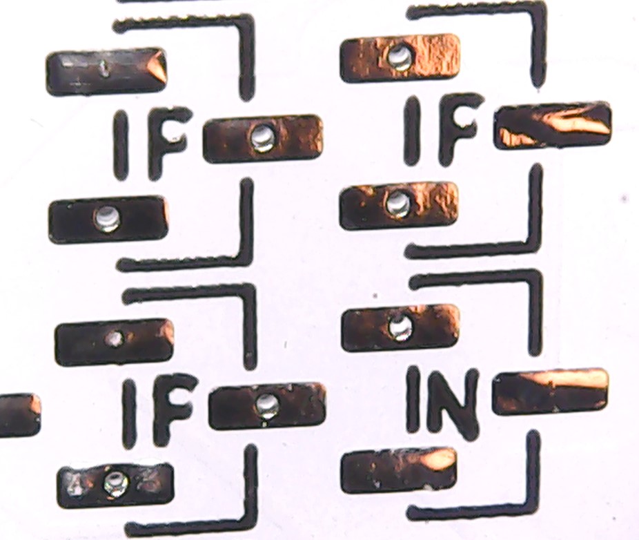
This also left the PCB outline clean so the black transistors would stand out over the white PCB and let the transistors themselves hide the silscreen.
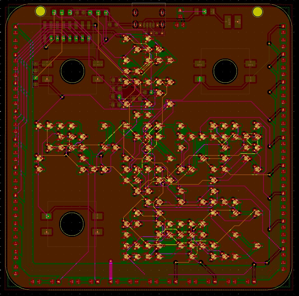
During the layout process it became obvious that a two layer PCB would not suffice. If I hadn’t wanted to connect the LEDs to the shift register, I would have achieved this on a 2 layer board, like the test ones. But the extra connections to the outside of the PCB, and the closer spacing of the transistors to form the QR code meant that this was not possible.
I populated the PCB by hand. I could get these populated at the PCB house, but I was still unsure they would work, and therefore didn’t want to risk the extra (and quite considerable) cost.
Unfortunately white two layer PCB’s come at a cost, but this extra cost is only small. Going to 4 layers also comes at a cost, but 4 layers AND white, Ouch!, Enough Ouch! for me not to want the extra cost in having the components placed for me as well.
Kicad’s ability to superimpose a reference graphic was also crucial in the layout of the PCB, I could have the QR code and the grid to place the transistors on the yellow dot, and ensure they were all correctly placed as below.
Soldering
The transistors (and other components) were placed by hand. I didn’t have a solder mask made for this (cost again), I used a solder paste syringe with a 0.5mm needle to apply the solder onto the pads and manually, then drop the transistor in place with a pair of tweezers. The population/soldering of the whole PCB took around 2.5 hours. Next time it will be faster, I learnt a lot.
It Works !
I tentatively powered it up, and it worked… First time, mostly, see: Errors.
Errors
I always try to admit to my errors, it proves that people are not 100% perfect like many portray on the internet.
I missed a wire driving the first LED as one page of the schematic had a label D0 and the other had a label D (there is a bodge wire on the PCB now, top right hand corner.)
Also this absolute classic, also now bodged on the PCB.
The Random mode using XOR feed back does not take its feed back from odd numbered LEDs as the phase of the clock is wrong.
It also occasionally loses a bit, only with XOR feedback, This will take a long time to debug.
Update: It did take a long time, it was a single dry (soldered) joint between two d-type latches. I was lucky, it got worse, making it easier to find.
Complete Schematics.
For anyone that would actually like the pain in duplicating this, or just for reference.