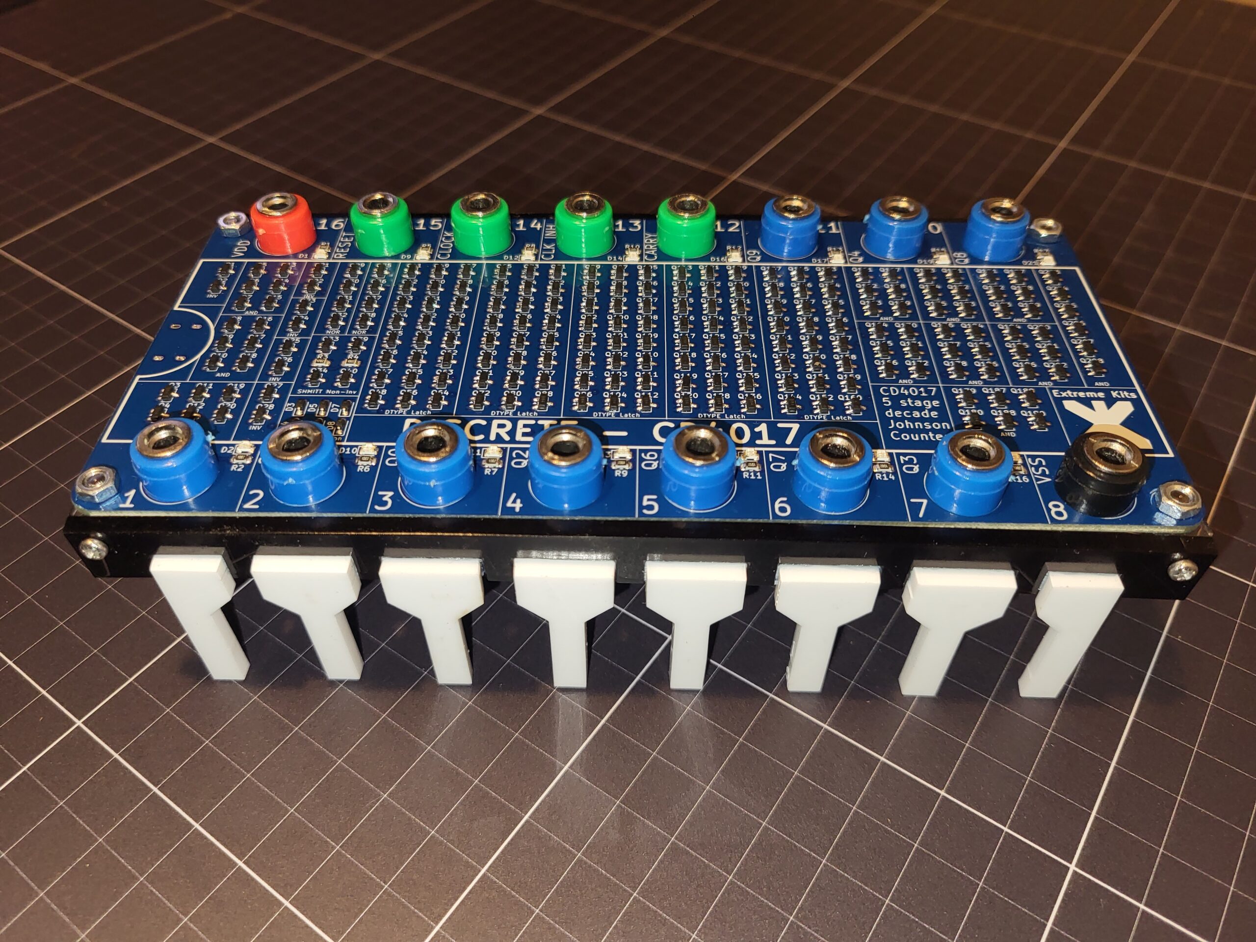
When I was young. CMOS and TTL chips were the building blocks of most of my digital projects.
As a good proportion of my non computer circuits had to run from batteries, CMOS was the series of choice as they would run from 3v (2 x 1.5v Cells) to 12v (a lead acid battery).
Making LEDs chase was a great learning exercise and by simply connecting a CD4017 to 10 LEDS and resistors, and using a simple oscillator to provide a clock pulse was a simple way to do this.
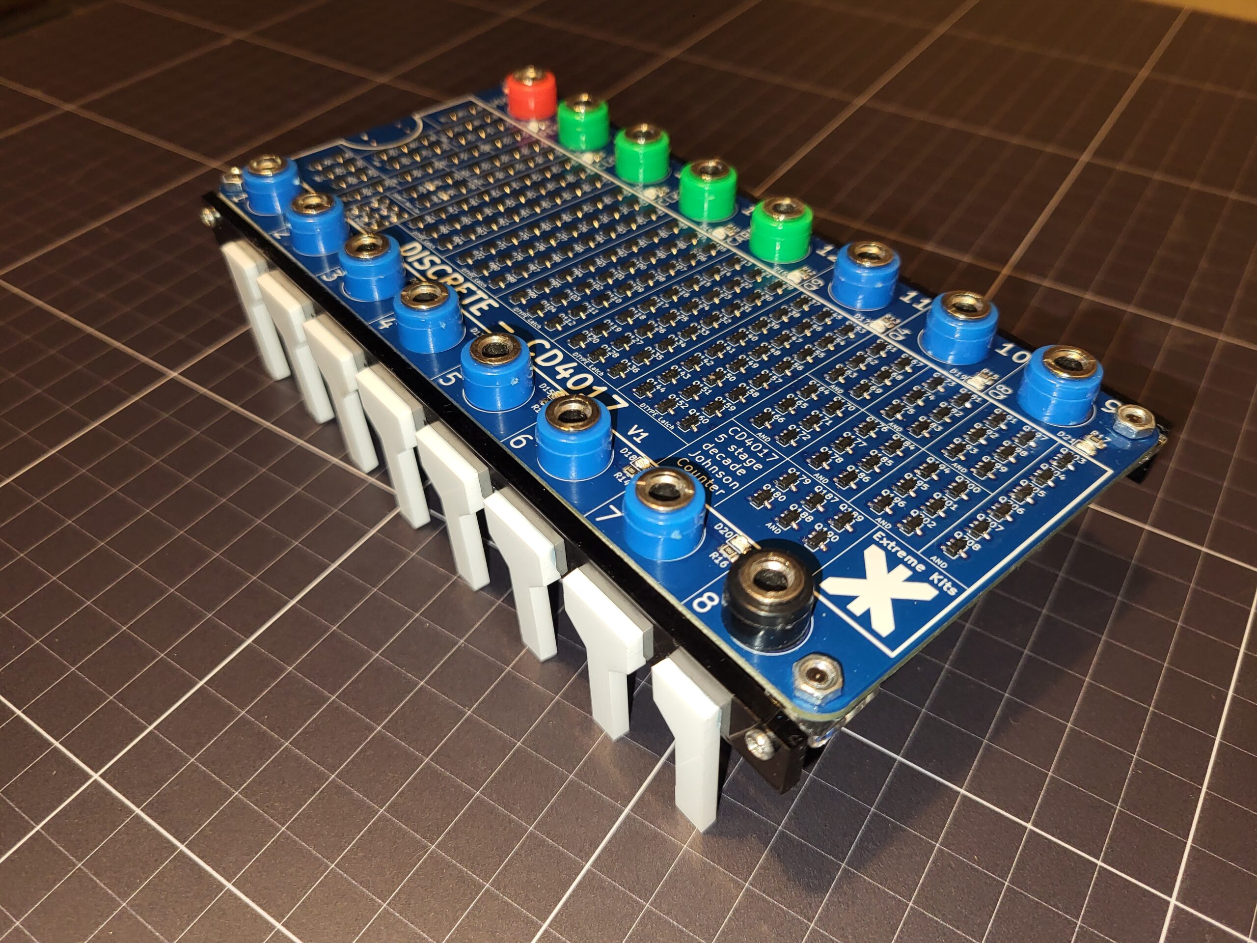
As my electronic circuits became more complicated they would regularly require some form of “do this”, “then do this “next ” form of control, and the CD4017 formed the heart of many circuits because of this.
CD4017 Primer
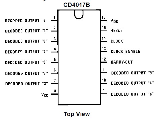
The CD4017 has 16 pins. Pin 16 is the positive power or VDD pin (3-18V) and pin 8 is ground, 0v or Vss power pin. We will assume that these are connected and powered in the rest of the description.
From the timing diagram below, the operation of the CD4017 can be seen. In modern terms it’s relatively simple
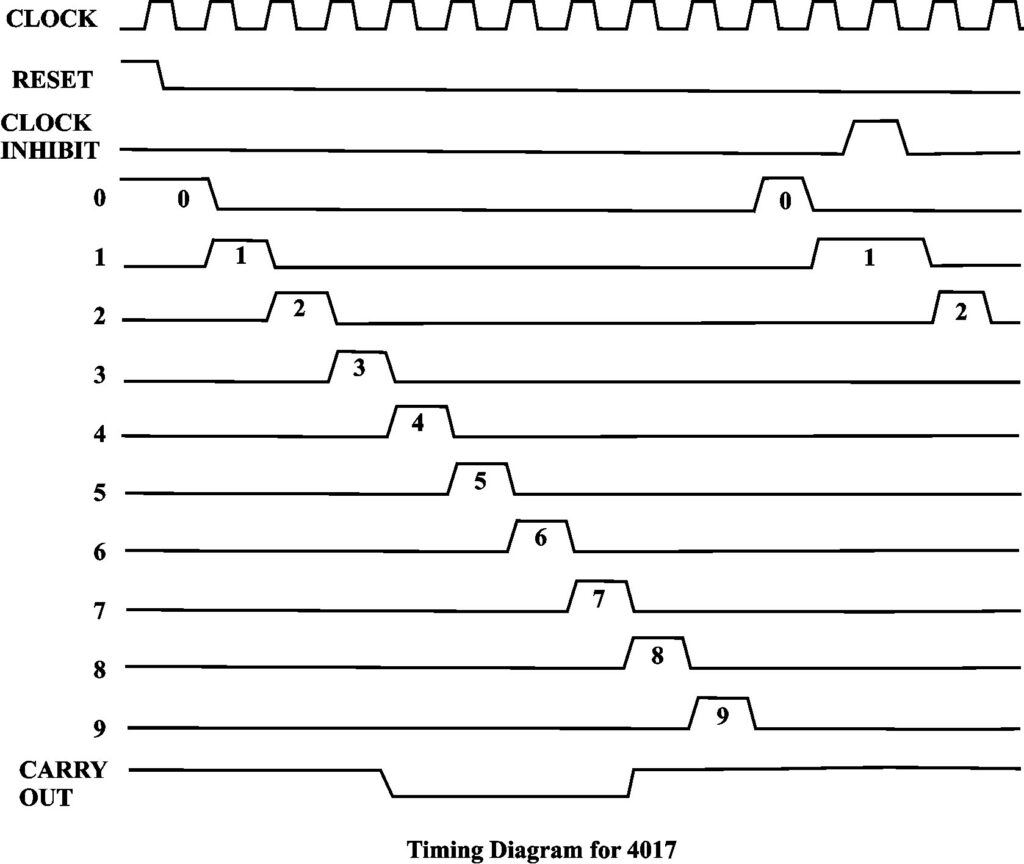
The clock input is a pulse train usually from an oscillator, or a button, or another IC, even another CD4017.
Assuming for now that the Clock Inhibit and Reset pins are held at 0v, for each +ve to 0v transition on the clock pin, the CD4017 will count up one.
The CD4017 has 10 outputs labelled Q0 to Q9. On power up, the Q0 output will be held high, and Q1-Q9 will be low. As the clock is pulsed, the CD4017 counts, and the output will change from Q0, to Q1 being made high, then Q2,Q3 etc in sequence, until after 10 pulses the counter rolls over to Q0 again.
The Reset line can be pulled high at any point, and this will restart the counter at Q0
The Clock inhibit line can be pulled high and this will stop the counting process, which will resume again when the line is returned to a low state.
The Carry out signal is low with Q0-Q4 and high with Q5-Q9. This enables it to be used to clock another CD4017, enabling the pair of them to count upto 99.
So, how is the CD4017 implemented with only transistors?
MOSFET Logic Primer
The MOSFET
We start witha simple MOSFET
A MOSFET is a switch
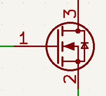
With this FET, an N-type, with 0 volts on the gate (1) the Drain(3) and the Source(2) will not be connected.
If you put a few volts +ve on the gate(1), the Drain(3) and the Source(2) will be connected.
There is also another type of FET, also a switch (note the arrow direction has changed on the symbol).
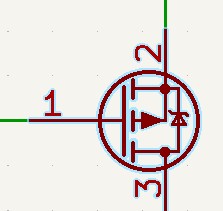
With this FET, a P-type, with 0 volts on the gate (1) the Drain(2) and the Source(3) will be connected.
If you put a few volts on the gate(1), the Drain(2) and the Source(3) will be disconnected.
(The P-type is actually an upside down N-type and you are actually putting -ve volts on the gate with respect to the source, but that makes the rest of the descriptions below really hard. https://en.wikipedia.org/wiki/Field-effect_transistor for more information)
The Inverter or NOT gate.
So, we can make the simplest type of logic gate with transistors, an inverter or NOT gate.
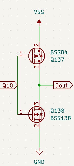
A NOR gate has one input and one output. A HIGH(1) on the input will give a LOW(0) on the output, and a LOW(0) on the input will make a HIGH(1) on the output.
| In | Out |
|---|---|
| 0 | 1 |
| 1 | 0 |
So, from the above description, If the input (Q10) it at GND (LOW), the bottom transistor (n-type) is OFF and the Top transistor(p-type) is ON.
As the top transistor is connected to VSS (HIGH) the output (Dout) is HIGH.
Making Q10 HIGH, Turns on the Bottom transistor which is connected to GND, and turns off the top transistor. So the output is LOW.
Confused. Yes, I have to think about this hard every time I come across it.
One thing to take from this simple example is, if you only have one transistor between the input and the output, the signal will be inverted.
This is the reason that all of the basic gates made from transistors are in their inverted forms, NAND, NOR etc, as you need another pair of transistors to invert the output again, to make the gates their non inverted counterparts OR and AND.
For more details on the way logic gates work take a look at this great guide https://www.geeksforgeeks.org/digital-logic/logic-gates/
From here, we can make all of the classic Gates, NOR,NAND and with the addition of an inverter gate as above OR and AND gates.
NAND (Not AND)
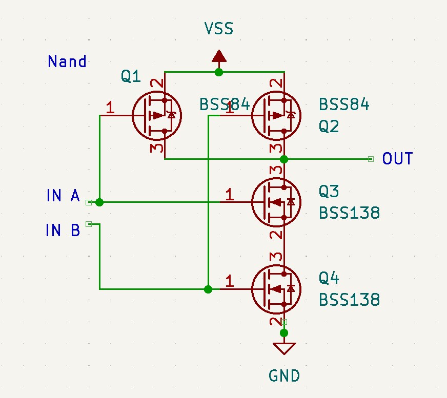
The NAND gate is slightly more complicated having two inputs and one output.
| A | B | OUT |
|---|---|---|
| 0 | 0 | 1 |
| 1 | 0 | 1 |
| 0 | 1 | 1 |
| 1 | 1 | 0 |
As Q3 and Q4 are N-Type only If both of the transistors have a HIGH(1) on their input, then the output will be pulled LOW(0). If either of the P-Type transistors Q1 and Q2 have a LOW(0) on their input then the output will be pulled HIGH(1)
NOR (Not Or)
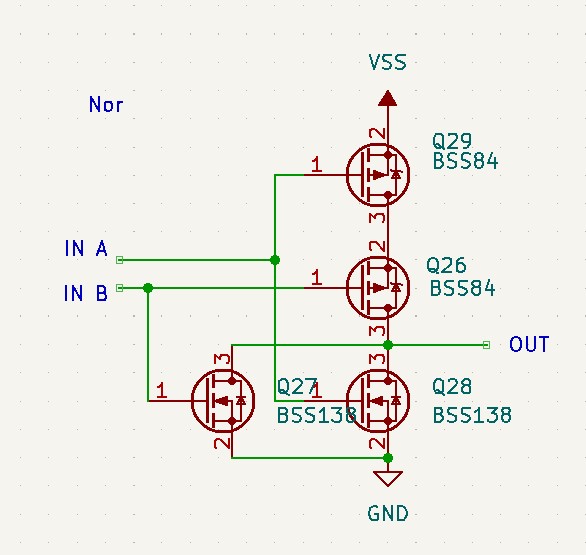
The NOR gate is similar also having two inputs and one output.
| A | B | OUT |
|---|---|---|
| 0 | 0 | 1 |
| 1 | 0 | 0 |
| 0 | 1 | 0 |
| 1 | 1 | 0 |
As Q27 and Q28 are N-Type If ether of the transistors have a HIGH(1) on their input, then the output will be pulled LOW(0). If both of the P-Type transistors Q26 and Q29 have a LOW(0) on their input then the output will be pulled HIGH(1)
The D-Type Latch
So, I needed to control a bunch of LEDS, my thought was a shift register. My idea was, if we make a long shift register from D-Type latches we can feed in a string of on’s and off’s, and it can filter through the shift register driving the LEDs. (https://www.geeksforgeeks.org/digital-logic/shift-registers-in-digital-logic/)
So First, a D-type latch circuit
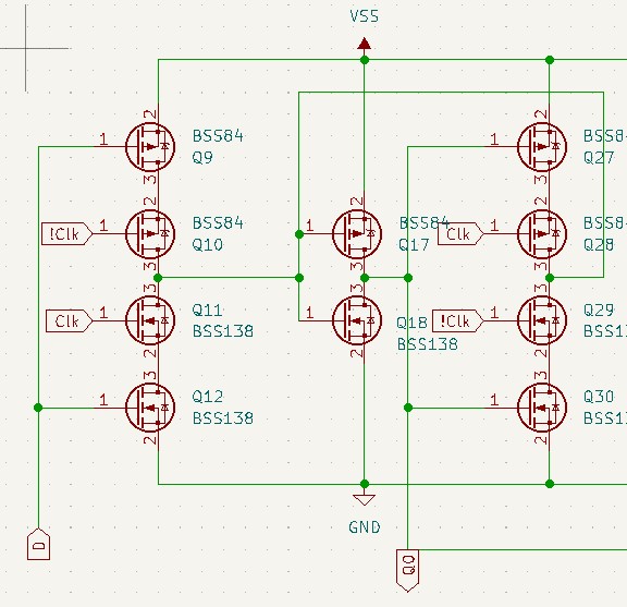
This takes a high or low (1, or 0) signal ‘D’, and stores it’s state at ‘Q0’ when there is a +ve going clock ‘Clk’. You can see that this circuit also uses the inverted clock ‘!Clk’.
For a 10 transistor circuit, it’s operation is really quite complicated. But basically on a +ve clock ‘D’ is connected to MOSFETs Q17 and Q18, setting the output ‘Q0’, this is latched during a -ve going clock by the MOSFETs Q27,Q28,Q29 and Q30 and the feedback loop back to MOSFETs Q17,Q18.
This works fine, but if you connect another d-type as above, connecting the new D to the output Q0, the signal gets latched immediately on the +ve going clock, so all subsequent D-types latch ‘on’ with the first clock transition, not what we need in a D-Type.
The solution, is to alternate a +ve latching D-type latches with a -ve latching D-type latches. This is easily achieved by swapping the ‘Clk’ and ‘!Clk’ signals in the second latch.
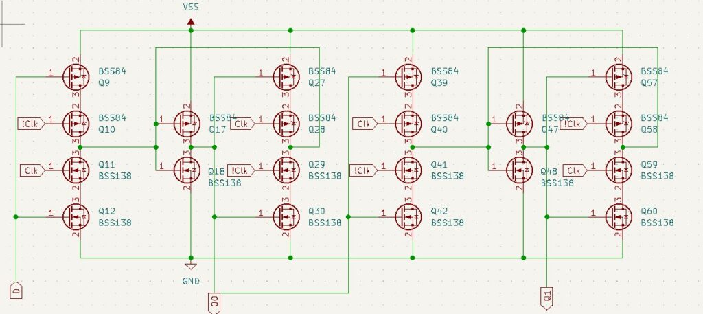
So these 20 transistors form a single Dtype FlipFlop in a shift register.
The discrete CD4017 has 5 of these stages which take up most of the 208 transistors.
The Logic Diagram
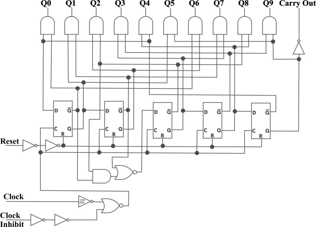
This is based on the logic diagram shown in the CD4017 datasheet, and clearly shows the IC is made from a number of logic gates.
The 5 Dtype-latch flip-flops are across the centre, and the decoding logic for the Q outputs and the Carry Out line are at the top of the diagram.
The 5 Dtype-latches count as a Johnson counter giving 5 outputs. These 5 outputs are then decoded into the 10 decimal outputs.
The Johnson counter counts as a shift register with an inverted feed back from the last stage to the first.
The count starts at 00000 then on the clock the last digit is inverted and fed into the first latch, the other digits are shifted right. The count becomes 10000, another clock gives 11000. This gives ten count stages as in the table below.
5 stage Johnson counter
| Latch 0 | Latch 1 | Latch 2 | Latch 3 | Latch 5 | Decimal (Q) output |
| 0 | 0 | 0 | 0 | 0 | 0 |
| 1 | 0 | 0 | 0 | 0 | 1 |
| 1 | 1 | 0 | 0 | 0 | 2 |
| 1 | 1 | 1 | 0 | 0 | 3 |
| 1 | 1 | 1 | 1 | 0 | 4 |
| 1 | 1 | 1 | 1 | 1 | 5 |
| 0 | 1 | 1 | 1 | 1 | 6 |
| 0 | 0 | 1 | 1 | 1 | 7 |
| 0 | 0 | 0 | 1 | 1 | 8 |
| 0 | 0 | 0 | 0 | 1 | 9 |
Carry out is taken as inverted from latch 5, as this goes through one cycle as the counter goes from 0 to 9. This enables another 4017 to use this as its clock, to count up when a complete cycle has completed.
Usage
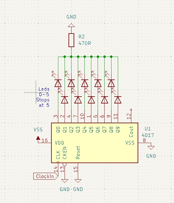
In its basic usage, Clock enable and Reset is earthed. A clock is provided on pin 14, for each pulse on this clock, the LEDs increment through Q0,Q1 …. Q9 and repeat.
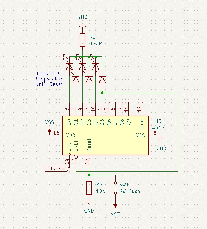
In this example, Clock enable is tied to Q5 and Reset is earthed via a resistor, but a push button will briefly connect it to Vss(+). A clock is provided on pin 14, for each pulse on this clock, the LEDs increment through Q0,Q1 …. Q5, when q5 is set the clock is disabled, and the counter will stop.
Pressing Reset, will re-enable the counting from Q0
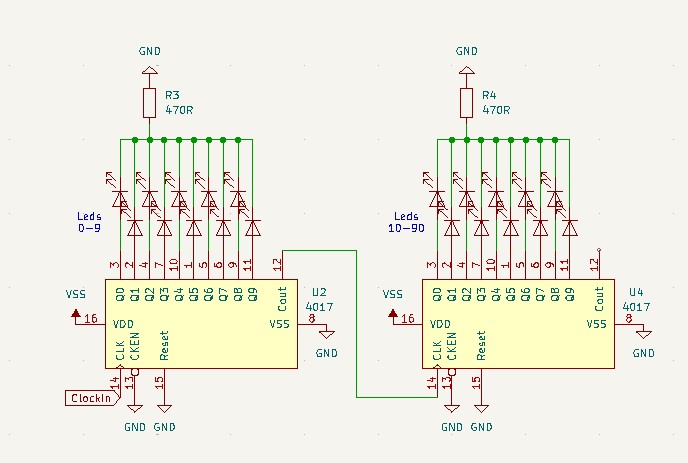
In this usage, Clock enable and Reset is earthed. A clock is provided on pin 14 of the first 4017. the second 4017 is clocked by the carry out line.
For each pulse on this clock, the LEDs increment through Q0,Q1 …. Q9 and repeat on the first 4017. The second 4017 will clock when a complete cycle is finished, giving a count of 0-99. with the first 4017 doing the single digits and the second the tens.
Resources
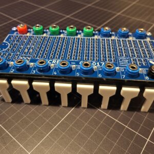
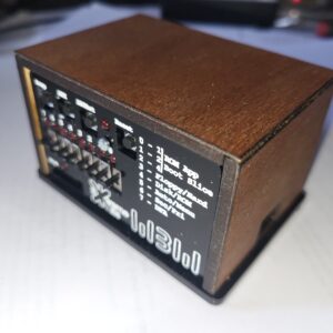
More details of the Discrete CD4017 is available in the resources section of extkits web site